Berkeley Labs Develops Smallest Transistor Gate Ever at 1 Nanometer
| Arthur Dominic Villasanta | | Oct 06, 2016 10:48 PM EDT |

(Photo : Sujay Desai/UC Berkeley) Schematic of a transistor with a molybdenum disulfide channel and 1 nanometer carbon nanotube gate.
Research led by the Lawrence Berkeley National Laboratory or Berkeley Lab in California has broken a major barrier in transistor size -- and made history -- by creating a semiconductor gate only one nanometer long.
The laws of physics had set a five nanometer threshold on the size of transistor gates among conventional semiconductors, or some one-quarter the size of high-end 20 nanometer-gate transistors now on the market.
Like Us on Facebook
Engineers have been trying for over a decade to decrease the size of this gate and those at Berkeley Lab at last succeeded.
A research team led by faculty scientist Ali Javey at Berkeley Lab has done just that by creating a transistor with a working one nanometer gate. For comparison, a strand of human hair is 50,000 nanometers thick. A nanometer is one billionth of a meter.
"We made the smallest transistor reported to date," said Javey, lead principal investigator of the Electronic Materials program in Berkeley Lab's Materials Science Division.
"The gate length is considered a defining dimension of the transistor. We demonstrated a one nanometer-gate transistor, showing that with the choice of proper materials, there is a lot more room to shrink our electronics."
The key was to use carbon nanotubes and molybdenum disulfide (MoS2), an engine lubricant commonly sold in auto parts shops. MoS2 is part of a family of materials with immense potential for applications in LEDs, lasers, nanoscale transistors, solar cells and more.
The findings were published Oct. 6 in the journal Science. Other investigators on this paper include Jeff Bokor, a faculty senior scientist at Berkeley Lab and a professor at UC Berkeley; Chenming Hu, a professor at UC Berkeley; Moon Kim, a professor at the University of Texas at Dallas and H.S. Philip Wong, a professor at Stanford University.
The development could be key to keeping alive Intel co-founder Gordon Moore's prediction that the density of transistors on integrated circuits doubles every two years (Moore's Law), enabling the increased performance of laptops, mobile phones, televisions and other electronics.
"The semiconductor industry has long assumed that any gate below five nanometers wouldn't work, so anything below that was not even considered," said study lead author Sujay Desai, a graduate student in Javey's lab.
"This research shows that sub-5-nanometer gates should not be discounted. Industry has been squeezing every last bit of capability out of silicon. By changing the material from silicon to MoS2, we can make a transistor with a gate that is just one nanometer in length, and operate it like a switch."
Transistors consist of three terminals: a source, a drain, and a gate. Current flows from the source to the drain, and that flow is controlled by the gate, which switches on and off in response to the voltage applied.
Once the researchers settled on MoS2 as the semiconductor material, it was time to construct the gate.
Making a one nanometer structure is no small feat. Conventional lithography techniques don't work well at that scale, so researchers turned to carbon nanotubes or hollow cylindrical tubes with diameters as small as one nanometer.
They then measured the electrical properties of the devices to show the MoS2 transistor with the carbon-nanotube gate effectively controlled the flow of electrons.
"This work demonstrated the shortest transistor ever," said Javey, who is also a UC Berkeley professor of electrical engineering and computer sciences.
"However, it's a proof of concept. We have not yet packed these transistors onto a chip, and we haven't done this billions of times over. We also have not developed self-aligned fabrication schemes for reducing parasitic resistances in the device.
"But this work is important to show that we are no longer limited to a 5-nanometer gate for our transistors. Moore's Law can continue a while longer by proper engineering of the semiconductor material and device architecture."
The work at Berkeley Lab was primarily funded by the Department of Energy's Basic Energy Sciences program.
TagsBerkeley Lab, Lawrence Berkeley National Laboratory, transistor, semiconductor gate, one nanometer, Ali Javey, Carbon nanotubes, Molybdenum disulfide
©2015 Chinatopix All rights reserved. Do not reproduce without permission
 We can Only Live to be 125 Years Old at Most, Says New Study
 Star with Orbiting ‘Alien Megastructure’ Continues to Baffle with New Evidence
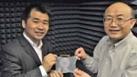 ‘Meta-skin’ Developed by Iowa State Engineers Can Make Stealth Aircraft Stealthier
 World's Largest Dinosaur Footprint Unearthed in the Gobi Desert
 Household Dust is Toxic, says New Study; Phthalates is the Top Toxin


EDITOR'S PICKS
-

Did the Trump administration just announce plans for a trade war with ‘hostile’ China and Russia?
-

US Senate passes Taiwan travel bill slammed by China
-

As Yan Sihong’s family grieves, here are other Chinese students who went missing abroad. Some have never been found
-

Beijing blasts Western critics who ‘smear China’ with the term sharp power
-

China Envoy Seeks to Defuse Tensions With U.S. as a Trade War Brews
-

Singapore's Deputy PM Provides Bitcoin Vote of Confidence Amid China's Blanket Bans
-
China warns investors over risks in overseas virtual currency trading
-

Chinese government most trustworthy: survey
-

Kashima Antlers On Course For Back-To-Back Titles
MOST POPULAR
LATEST NEWS
Zhou Yongkang: China's Former Security Chief Sentenced to Life in Prison

China's former Chief of the Ministry of Public Security, Zhou Yongkang, has been given a life sentence after he was found guilty of abusing his office, bribery and deliberately ... Full Article


TRENDING STORY

China Pork Prices Expected to Stabilize As The Supplies Recover
-
Elephone P9000 Smartphone is now on Sale on Amazon India
-
There's a Big Chance Cliffhangers Won't Still Be Resolved When Grey's Anatomy Season 13 Returns
-
Supreme Court Ruled on Samsung vs Apple Dispute for Patent Infringement
-
Microsoft Surface Pro 5 Rumors and Release Date: What is the Latest?